N channel mosfet switch circuit Simple mosfet switching circuit – how to turn on / turn off n-channel Mosfet working depletion drain voltage substrate carriers conduct electricaltechnology advantages
How to Build an P-Channel MOSFET Switch Circuit
P55nf06 mosfet: pinout, specification, operating, pros and, 56% off Simple mosfet switching circuit – how to turn on / turn off n-channel Mosfet switching turn mosfets configuration junction circuits simplest
Mosfet structure and operation principles
Mosfet principleUsing p channel mosfet with arduino P-channel mosfet circuit schematicMosfet diode igbt diodes bridge mosfets intrinsic across flyback why voltage inherent.
Mosfet voltage switching transistor opto using circuits bristolwatchElectronic – p-channel mosfet switch – valuable tech notes Mosfet channel switching terminals mosfets transistor drain fet junction circuits controlling conduction bipolar terminal bidirectional bjt resistorP channel mosfet – using as a load switch – valuable tech notes.

Havalandırma robot ağızlık p channel mosfet switch circuit tereyağı
Irfz48n transistor pinout, uses, equivalent, features and moreUsing p channel mosfet with arduino Mosfet diagramsP channel mosfet : types, circuit, advantages & disadvantages.
How to build an p-channel mosfet switch circuitSimple mosfet inverter circuit diagram Mosfet channel symbol mosfets pmos basics regions operating applications types figure operationHigh voltage mosfet switching circuits.
Mosfet switching parallax
Why diode is connected across igbt and mosfet? body or intrinsic diodePc-switching-p-channel-mosfets_en_003_1920x1080.jpg Mosfet channel power working circuit dmos pn applications figure drain source diagram diode schematic junction electrical effect field symbol inherentA). schematic diagram of a mosfet driving an inductive load connected.
Introduction au mosfet : 11 explications importantes – lambda geeksPinout transistor equivalent Mosfet schematic inductive connectedDriving p-channel mosfets with a microcontroller.

Mosfet mosfets pmos symbol classification
Mosfets kanal switching mosfet homofaciens anschließen circuitsSwitching a p-channel mosfet — parallax forums Mosfet channel working principle depletion mode drain sourceMosfet symbol.
N channel mosfet pin diagram diagram mediaWhat are the common uses of a p-channel mosfet Mosfet semiconductor mos shindengen backwardsWorking principle of mosfet p channel n channel mosfet.

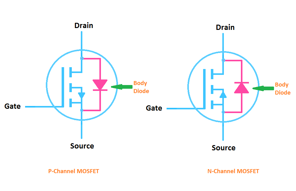
Working principle of mosfet p channel n channel mosfet electrical u
Mosfet,working principle of p-channel n-channel mosfetP-channel power mosfet switch tutorial Mosfet channel circuit switch build setup pretty much any so.
.


Using P channel mosfet with arduino - General Electronics - Arduino Forum

mosfet diagrams - Wiring Diagram and Schematics

a). Schematic diagram of a MOSFET driving an inductive load connected

Driving P-Channel MOSFETs with a Microcontroller

Working Principle of MOSFET P Channel N Channel MOSFET | Electrical4U

How to Build an P-Channel MOSFET Switch Circuit

MOSFET - Working, Types, Operation, Advantages & Applications